Wafer scale 2D magnetic material growth method explained through IISc breakthrough in scalable 2D magnetic materials synthesis for spintronics and electronics.
Introduction: A Major Leap in 2D Magnetic Material Science
The scientific community is witnessing a transformative advancement in material science with the announcement from the Indian Institute of Science (IISc), Bengaluru. Researchers have successfully demonstrated wafer-scale growth of 2D magnetic materials, marking a significant milestone in next-generation electronics and quantum technologies.
At the heart of this innovation lies the wafer scale 2d magnetic material growth method explained, which showcases how large-area, high-quality thin films of chromium-based compounds can be produced using advanced deposition techniques. This breakthrough addresses long-standing challenges in scalability, stability, and industrial application of 2D magnetic systems.
The wafer scale 2d magnetic material growth method explained is not just a laboratory success—it represents a pathway toward commercial spintronics devices, ultra-sensitive sensors, and energy-efficient computing systems. Researchers emphasize that the wafer scale 2d magnetic material growth method explained could redefine how future electronic devices are fabricated.
Breakthrough at IISc and Its Global Importance
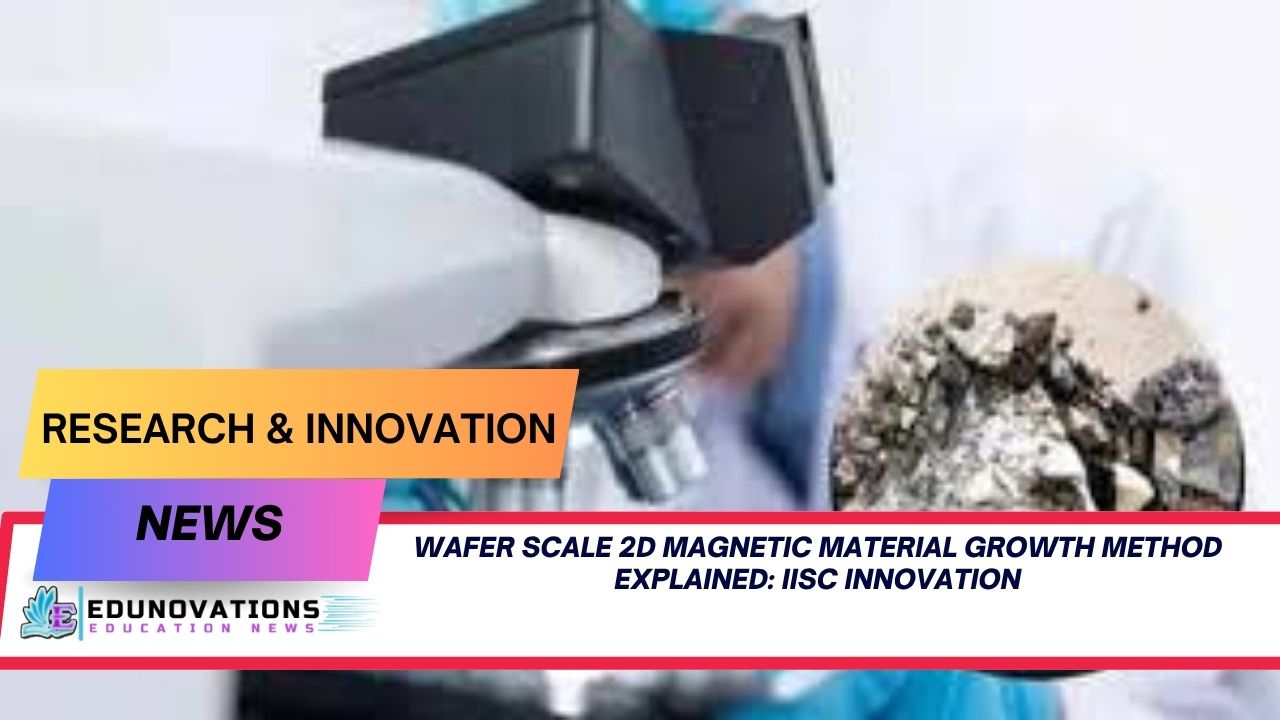
The IISc research team has developed a controlled process to grow chromium chloride (CrCl₃) thin films on mica substrates using Physical Vapour Transport Deposition (PVTD). This allows uniform growth over wafer-sized surfaces, a critical requirement for industrial scalability.
The wafer scale 2d magnetic material growth method explained in this study demonstrates how magnetic ordering can be preserved even at atomic thickness levels. Traditionally, 2D materials suffer from instability and environmental degradation, but this method significantly improves reliability.
Experts in nanotechnology highlight that the wafer scale 2d magnetic material growth method explained represents a shift from small-area experimental samples to industry-ready production techniques.
According to materials scientists, achieving wafer-scale uniformity is essential for integrating 2D materials into semiconductor manufacturing pipelines. The wafer scale 2d magnetic material growth method explained provides a scalable solution for this long-standing limitation.
Understanding 2D Magnetic Materials and Their Potential
Two-dimensional magnetic materials are atomically thin structures that exhibit magnetic properties at nanoscale thicknesses. These materials are crucial for:
- Spin-based electronics (spintronics)
- Quantum computing components
- Low-power memory devices
- Ultra-sensitive magnetic sensors
The wafer scale 2d magnetic material growth method explained shows how such materials can now be produced in large quantities without losing their magnetic integrity.
One of the key materials used in this research is chromium chloride (CrCl₃), which exhibits unique layered magnetic properties. Through the wafer scale 2d magnetic material growth method explained, researchers successfully stabilized its structure across large surfaces.
The ability to scale these materials is what makes the wafer scale 2d magnetic material growth method explained particularly significant for industrial adoption.
Physical Vapour Transport Deposition (PVTD) Technique
A critical part of the innovation is the PVTD method used for film deposition. This technique allows precise control over material vaporization and deposition, ensuring uniform crystal growth.
The wafer scale 2d magnetic material growth method explained relies heavily on PVTD to achieve consistent thickness across wafer surfaces. This ensures that the electronic and magnetic properties remain uniform throughout the material.
Researchers emphasize that the wafer scale 2d magnetic material growth method explained using PVTD can be adapted for other 2D materials as well, opening new research possibilities.
The scalability achieved through this process is a defining feature of the wafer scale 2d magnetic material growth method explained, making it suitable for semiconductor integration.
Role of Substrates in Material Stability
Mica substrates play a crucial role in stabilizing the thin films during growth. These substrates provide an atomically flat surface, which is essential for high-quality material formation.
The wafer scale 2d magnetic material growth method explained highlights how mica ensures minimal structural defects during deposition. This improves both performance and durability of the material.
Scientists note that without such substrates, the wafer scale 2d magnetic material growth method explained would not achieve the required uniformity at scale.
Applications in Spintronics and Future Electronics
One of the most promising applications of this research is spintronics—a technology that uses electron spin rather than charge for computation.
The wafer scale 2d magnetic material growth method explained enables the production of materials that can efficiently manipulate spin states. This could lead to:
- Faster processors
- Lower energy consumption devices
- High-density data storage systems
Experts believe that the wafer scale 2d magnetic material growth method explained will accelerate the transition from traditional silicon-based electronics to quantum-enhanced systems.
By enabling scalable production, the wafer scale 2d magnetic material growth method explained bridges the gap between laboratory research and industrial application.
Challenges Addressed by the IISc Innovation
Before this breakthrough, researchers faced several challenges:
- Material degradation when exposed to air
- Difficulty in scaling up production
- Lack of uniform magnetic properties
- Instability in thin-layer formation
The wafer scale 2d magnetic material growth method explained directly addresses these issues by improving stability and scalability.
One of the most significant achievements of the wafer scale 2d magnetic material growth method explained is maintaining magnetic order across large wafer surfaces without structural defects.
This advancement is expected to inspire further innovations in 2D material engineering worldwide.
Expert Insights and Scientific Reactions
Leading scientists in condensed matter physics have praised IISc’s achievement. According to research experts, the wafer scale 2d magnetic material growth method explained is a “game-changer for scalable quantum material fabrication.”
Dr. Ashok Kumar, a materials science researcher, noted that such developments are crucial for bridging the gap between theoretical physics and industrial applications.
The wafer scale 2d magnetic material growth method explained is also being seen as a stepping stone toward room-temperature quantum devices.
International research communities are closely monitoring this development, as the wafer scale 2d magnetic material growth method explained could influence global semiconductor strategies.
Integration with Digital Learning and Research Platforms
Educational institutions and research platforms can benefit from this advancement by incorporating updated materials science modules.
Students can explore related concepts through:
- https://courses.edunovations.com/ (NCERT Courses)
- https://edunovations.com/notes/ (Academic Notes)
- https://edunovations.com/currentaffairs/ (Latest Science Updates)
- https://edunovations.com/mcq/ (Practice Questions)
- https://edunovations.com/videos/ (Learning Videos)
The wafer scale 2d magnetic material growth method explained can also be used as a case study in advanced physics and nanotechnology courses.
Institutions aiming to improve digital infrastructure can explore solutions from https://www.martindiainfotech.com/ for academic and research websites.
Future Prospects of 2D Magnetic Material Research
The future of electronics will likely depend heavily on scalable nanomaterials. The wafer scale 2d magnetic material growth method explained provides a strong foundation for this transition.
Potential developments include:
- Quantum memory devices
- Energy-efficient AI chips
- Advanced biomedical sensors
- Ultra-thin flexible electronics
Researchers believe that the wafer scale 2d magnetic material growth method explained will inspire new industrial collaborations globally.
With continued research, the wafer scale 2d magnetic material growth method explained could become a standard manufacturing process in advanced electronics industries.
Conclusion
The IISc breakthrough in wafer-scale growth of 2D magnetic materials represents a major step forward in nanotechnology and materials science. The wafer scale 2d magnetic material growth method explained highlights how scientific innovation can move from experimental setups to real-world applications.
By solving critical challenges in scalability and stability, the wafer scale 2d magnetic material growth method explained opens doors to revolutionary technologies in computing, sensing, and quantum systems.
As research continues, the wafer scale 2d magnetic material growth method explained is expected to play a central role in shaping the future of electronics and material engineering.
Toppers Use Mind Maps to score more than 95%
NCERT Class 11th Commerce Mind Maps
Add to cartOriginal price was: ₹999.00.₹199.00Current price is: ₹199.00.NCERT Class 12th Chemistry Mind Maps
Add to cartOriginal price was: ₹199.00.₹75.00Current price is: ₹75.00.NCERT Class 12th Commerce Mind Maps
Add to cartOriginal price was: ₹999.00.₹199.00Current price is: ₹199.00.NCERT Class 12th Science Mind Maps
Add to cartOriginal price was: ₹999.00.₹199.00Current price is: ₹199.00.NCERT Mind Maps For Class 10th
Add to cartOriginal price was: ₹999.00.₹199.00Current price is: ₹199.00.


Purchase Today
FAQs
1. What is wafer scale 2d magnetic material growth method explained in simple terms?
It refers to a scalable technique used to grow large-area 2D magnetic thin films for electronic applications.
2. How does PVTD help in wafer scale 2d magnetic material growth method explained?
PVTD ensures uniform vapor deposition, which is essential in the wafer scale 2d magnetic material growth method explained.
3. Why is chromium chloride important in wafer scale 2d magnetic material growth method explained?
CrCl₃ is a key material used for its stable magnetic properties in thin-film applications.
4. What role do substrates play in wafer scale 2d magnetic material growth method explained?
Substrates like mica provide a stable base for uniform film growth.
5. How is wafer scale 2d magnetic material growth method explained useful in spintronics?
It enables scalable production of materials that control electron spin for faster devices.
6. Can wafer scale 2d magnetic material growth method explained be used commercially?
Yes, it has strong potential for industrial-scale electronic device manufacturing.
7. What are the challenges solved by wafer scale 2d magnetic material growth method explained?
It solves issues like instability, scalability, and non-uniform material growth.
8. How does IISc contribute to wafer scale 2d magnetic material growth method explained research?
IISc developed the core experimental framework for this breakthrough.
9. What future technologies depend on wafer scale 2d magnetic material growth method explained?
Quantum computing, AI chips, and ultra-efficient electronics.
10. Is wafer scale 2d magnetic material growth method explained important for students?
Yes, it is a key concept in nanotechnology and advanced materials science studies.