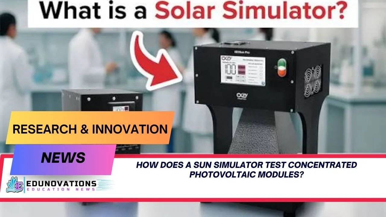
Discover how does a sun simulator test concentrated photovoltaic modules as IIT Kanpur and NexPV partner to build India’s first CPV testing facility.
In a landmark step toward strengthening sovereign clean energy infrastructure, the Indian Institute of Technology Kanpur (IIT Kanpur) has signed a Memorandum of Understanding (MoU) with Bengaluru-headquartered deep-tech firm NexPV Energy Systems. Facilitated by Invariance Automation—a member company of IIT Kanpur’s Research and Technology Park Foundation (Technopark@iitk)—this strategic industry-academia partnership aims to design and engineer India’s first end-of-line testing facility for advanced solar hardware. As clean energy researchers refine next-generation technology, a critical question arises for quality assurance engineers: how does a sun simulator test concentrated photovoltaic modules when traditional testing methods fall short?
The primary objective of this project is to fill a massive technical gap in India’s renewable energy manufacturing ecosystem. While standard solar panel testing facilities are widely available across the subcontinent, Specialized testing infrastructure tailored specifically for Concentrated Photovoltaic (CPV) architecture does not currently exist in the nation. By combining high-precision academic research with industrial manufacturing scale, this project accelerates India’s net-zero transition targets for 2070 and bolsters sovereign technological self-reliance.
Understanding how does a sun simulator test concentrated photovoltaic modules requires analyzing how these advanced clean tech systems interact with concentrated solar radiation, optical lenses, and precise spectral alignment.
Unpacking the Engineering Behind Concentrated Photovoltaic Systems
Conventional photovoltaic (PV) solar panels rely on broad silicon wafers that directly capture both direct and diffuse sunlight. While silicon solar panels have successfully powered millions of homes globally, they face inherent thermodynamic efficiency limits, usually capping practical module efficiency between 18% and 23%. Additionally, traditional silicon panels demand massive physical surface areas and extensive land footprints to generate megawatt-scale power.
Concentrated Photovoltaic (CPV) systems bypass these physical limitations by utilizing specialized optical lenses—such as Fresnel lenses or parabolic mirrors—to focus direct sunlight onto tiny, highly efficient solar cells. Rather than using broad silicon sheets, CPV technology relies on advanced multi-junction solar cells composed of stacked III-V semiconductor materials (such as Indium Gallium Phosphide, Indium Gallium Arsenide, and Germanium).
                                  CONCENTRATED PHOTOVOLTAIC (CPV) DESIGN
                                 ========================================

       [ Sunlight Rays ]                     [ Focused Light Cone ]                  [ Stacked Cell Architecture ]
    |   |   |   |   |   |                      \                /                     +-----------------------+
    V   V   V   V   V   V                       \              /                      | InGaP Layer (Top)     | -> Captures High Energy
  +-----------------------+                      \            /                       +-----------------------+
  |    Optical Lens       |   =================>  \          /    =================>  | InGaAs Layer (Middle) | -> Captures Mid Energy
  |   (Fresnel / Mirror)  |                         \      /                          +-----------------------+
  +-----------------------+                          \    /                           | Ge Layer (Bottom)     | -> Captures Infrared
                                                      \  /                            +-----------------------+
                                                       \/                             |  Cell Area: < 0.1%    | -> Cuts silicon usage >99%
                                                  [ Micro Cell ]                      +-----------------------+
Because these specialized multi-junction units capture multiple segments of the solar spectrum simultaneously, their theoretical energy conversion efficiency exceeds 40%. The optical lenses concentrate light by hundreds of times onto cells that occupy less than 0.1% of the total panel surface area. Consequently, CPV technology slashes raw semiconductor material requirements by more than 99% compared to conventional flat-plate modules.
Students and engineering candidates preparing for technical entrance examinations can review fundamental semiconductor physics principles through NCERT Courses to better understand multi-junction bandgap engineering.
Technical Comparison: Standard vs. CPV Testing Needs
To evaluate why specialized laboratory equipment is necessary, we must examine the difference between cpv sun simulator and flat plate solar simulator equipment. Standard flat-plate solar panels absorb ambient, scattered, and diffuse light from all sky angles. Therefore, conventional flash solar simulators produce wide-angle light beam patterns designed to illuminate broad silicon surfaces uniformly.
+------------------------------------+--------------------------------------------------+--------------------------------------------------+
| Technical Feature                  | Standard Flat-Plate Solar Simulator              | CPV Sun Simulator                                |
+------------------------------------+--------------------------------------------------+--------------------------------------------------+
| Light Beam Divergence              | Wide angle / Divergent illumination              | Highly collimated (Parallel rays < 0.5 degrees)  |
| Solar Spectrum Match               | Standard AM1.5G (Global Spectrum)                | Precise AM1.5D (Direct Normal Irradiance)        |
| Light Source Sensitivity           | Accepts diffuse and ambient room light           | Strict rejection of off-axis scattered light     |
| Target Material                    | Single-junction Silicon Wafers                   | Multi-junction III-V Semiconductors              |
| Spectral Tuning Capabilities       | Single broad spectrum flash                      | Multi-channel LED/Xenon spectral control         |
+------------------------------------+--------------------------------------------------+--------------------------------------------------+
In stark contrast, CPV optics function exclusively when exposed to Direct Normal Irradiance (DNI)—direct, parallel sunlight coming straight from the sun’s disk. If light hits a CPV module at an angle off by even half a degree, the internal optics fail to focus the light onto the micro-cell target, causing power output to drop toward zero.
Furthermore, multi-junction cells inside CPV modules are connected in series. The overall current generated by the cell is constrained by whichever semiconductor layer receives the least amount of usable light. Therefore, a specialized CPV testing apparatus must reproduce the exact spectral distribution of direct sunlight across all wavelengths. This ensures that researchers can measure individual current outputs accurately without triggering current-mismatch bottlenecks during factory quality audits.
Engineers wanting to practice quantitative problems on photovoltaic bandgaps can check dedicated MCQ’s for hands-on practice.
The IIT Kanpur and NexPV Strategic Alliance
The collaborative project at IIT Kanpur is led by Professor Ashish Garg and his research team within the Department of Sustainable Energy Engineering. Professor Garg, a distinguished scholar in functional materials and clean energy technologies, emphasized the critical strategic role that testing infrastructure plays in national clean energy goals:
“India’s net-zero commitment for 2070 will require solar deployment at a scale far beyond today’s, and that growth must rest on domestic capability across the value chain. Testing infrastructure is a strategic part of that chain: a technology cannot scale if it cannot be measured reliably. CPV modules behave fundamentally differently from flat panels, and building India’s first simulator designed for them is exactly the kind of translational research IIT Kanpur is committed to.”
— Prof. Ashish Garg, Head of Sustainable Energy Engineering, IIT Kanpur
On the industrial side, Bengaluru-based NexPV Energy Systems, spearheaded by Director Chidananda Murthy R, brings deep operational expertise in CPV manufacturing. NexPV has spent three years operating proof-of-concept CPV systems in real-world desert conditions with high Direct Normal Irradiance.
                                  INDUSTRY-ACADEMIA COLLABORATION ECOSYSTEM
                                 ===========================================

       +-----------------------+              +-----------------------+              +-----------------------+
       |      IIT Kanpur       |              | NexPV Energy Systems  |              | Invariance Automation |
       | (Sustainable Energy)  |              |  (Industry Partner)   |              |  (Technopark@iitk)    |
       +-----------+-----------+              +-----------+-----------+              +-----------+-----------+
                   |                                      |                                      |
                   | R&D & Optical                        | Field Proof-of-Concept               | Commercialization &
                   | Engineering                          | & Manufacturing Scale                | Prototype Scaling
                   +--------------------------+-----------+--------------------------------------+
                                              |
                                              V
                               +------------------------------+
                               | High-Precision CPV Testing   |
                               | Infrastructure for India     |
                               +------------------------------+
Commenting on the necessity of local testing facilities to address domestic supply chain mandates, Chidananda Murthy R stated:
“India has crossed 168 GW of installed solar capacity, but domestic cell manufacturing remains well behind module capacity, and with the cell mandate now in force, that gap directly affects deployment. CPV needs less than one per cent of the cell area of a conventional panel and, in our systems, about half the land. It can open a new pathway for solar in India’s high-DNI regions. A domestic CPV simulator gives us the quality assurance to manufacture at scale.”
— Chidananda Murthy R, Director, NexPV Energy Systems
In variance Automation, a core incubate company within Technopark@iitk, serves as the commercialization and manufacturing bridge, ensuring that laboratory prototypes transition into commercial end-of-line testing equipment for solar factories.
Educators, research scholars, and academic institutions seeking digital outreach solutions or customized web portals can explore web design services by contacting Mart Ind Infotech.
Mechanics: How a Sun Simulator Tests CPV Modules Step-by-Step
Understanding how does a sun simulator test concentrated photovoltaic modules in a factory environment involves several precise optical and electrical calibration steps:
- Collimated Light Generation: The sun simulator uses a specialized optical lens array combined with high-intensity pulsed Xenon flash lamps or tuned LED matrices. This setup produces parallel light beams with a divergence angle of less than 0.5 degrees, recreating the direct parallel sunlight received from the sun.
- Spectral Matching (AM1.5D): The testing chamber filters light to mirror the Air Mass 1.5 Direct (AM1.5D) spectrum. This guarantees that top (InGaP), middle (InGaP/InGaAs), and bottom (Ge) semiconductor junctions absorb exact ratio proportions of photon energy.
- Precision Optical Alignment: The CPV module is mounted onto a dual-axis positioning stage. Automated sensors verify that the incoming collimated light beam aligns perfectly perpendicular to the module’s primary optical array.
- Pulsed Flash Measurement: The simulator fires high-intensity light pulses lasting between a few milliseconds and several hundred milliseconds. Flash testing minimizes thermal buildup, allowing accurate electrical measurement at a controlled standard testing temperature of 25°C.
- Data Acquisition & I-V Curve Mapping: High-speed data acquisition channels measure current-voltage (I-V) response curves across variable loads. The system extracts critical metrics, including Open-Circuit Voltage ($V_{oc}$), Short-Circuit Current ($I_{sc}$), Maximum Power Point ($P_{mp}$), and Fill Factor ($FF$).
                      CPV MODULE SUN SIMULATOR TESTING WORKFLOW
                     ===========================================

   +---------------------------------------------------------------------------------+
   | STEP 1: Collimated Light Generation                                             |
   | Light source produces ultra-parallel rays with beam divergence angle < 0.5°     |
   +---------------------------------------------------------------------------------+
                                           |
                                           V
   +---------------------------------------------------------------------------------+
   | STEP 2: AM1.5D Spectral Tuning                                                  |
   | Spectral filters balance photon energy across UV, Visible, and Infrared bands   |
   +---------------------------------------------------------------------------------+
                                           |
                                           V
   +---------------------------------------------------------------------------------+
   | STEP 3: Automated Dual-Axis Optical Alignment                                   |
   | Precision stage adjusts CPV module position to hit internal optical focal points|
   +---------------------------------------------------------------------------------+
                                           |
                                           V
   +---------------------------------------------------------------------------------+
   | STEP 4: Pulsed Flash & Temperature Control                                      |
   | Millisecond light pulse eliminates heat accumulation during measurement          |
   +---------------------------------------------------------------------------------+
                                           |
                                           V
   +---------------------------------------------------------------------------------+
   | STEP 5: High-Speed I-V Curve Mapping & Output Analytics                        |
   | Sensors record Voc, Isc, Pmp, and Fill Factor for production quality control   |
   +---------------------------------------------------------------------------------+
For students analyzing energy technology policies, reviewing updated Current Affairs resources provides broader national policy context around India’s renewable energy goals.
Land and Silicon Conservation Advantages
A primary driver behind CPV deployment is its exceptional efficiency regarding land use and critical raw materials. As solar deployment scales rapidly across Western India, land acquisition costs and environmental constraints in semi-arid regions present growing challenges for project developers.
                       RESOURCE REQUIREMENTS: CONVENTIONAL VS. CPV
                      =============================================

   Land Footprint Needed per MW                       Cell Material Area Required
   +---------------------------------------+          +---------------------------------------+
   | Standard PV: [████████████████] 100%  |          | Standard PV: [████████████████] 100%  |
   | CPV Solar:   [████████] ~50%          |          | CPV Solar:   [█] < 1%                 |
   +---------------------------------------+          +---------------------------------------+
As highlighted by industry studies on how concentrated photovoltaic cells reduce land and cell usage, CPV systems offer clear spatial advantages:
- Over 99% Reduction in Silicon/Semiconductor Area: By utilizing optical concentration ratios ranging from 300x to 1000x, CPV systems require less than 1% of the active semiconductor material needed by conventional silicon panels for equivalent power output.
- 50% Reduction in Land Usage: Dual-axis trackers keep CPV arrays elevated off the ground, allowing dual land use like agriculture or grazing while cutting total project land footprint by nearly half compared to fixed-tilt silicon arrays.
- Superior Performance in High-DNI Zones: In high Direct Normal Irradiance regions like Rajasthan, Gujarat, and Ladakh, high-efficiency CPV systems generate substantially higher daily kilowatt-hour yields per installed peak capacity.
Students researching sustainable infrastructure design can download reference material from comprehensive Notes libraries.
Overcoming Multi-Junction Cell Testing Challenges
Evaluating multi-junction cells presents unique technical hurdles during quality assurance tests. To understand what is multi junction cell testing in cpv solar modules, one must examine how stacked semiconductor layers operate in electrical series.
                         MULTI-JUNCTION CELL SPECTRAL HARVESTING
                        =========================================

       Solar Wavelength Spectrum                          Semiconductor Layer Absorber
   +---------------------------------+                +---------------------------------+
   | Short Wavelengths (300-660 nm)  | -------------> | Top Layer: InGaP Bandgap        |
   +---------------------------------+                +---------------------------------+
   | Medium Wavelengths (660-890 nm) | -------------> | Middle Layer: InGaAs Bandgap    |
   +---------------------------------+                +---------------------------------+
   | Near Infrared (890-1450 nm)     | -------------> | Bottom Layer: Germanium Substrate|
   +---------------------------------+                +---------------------------------+
In a triple-junction solar cell, each layer absorbs a specific light wavelength range:
- Top Junction (InGaP): Captures high-energy ultraviolet and blue light photons.
- Middle Junction (InGaAs): Absorbs visible and near-infrared light wavelengths.
- Bottom Junction (Germanium): Captures longer infrared light wavelengths.
Because these three junctions are connected in series, current flowing through the cell is limited by whichever junction produces the lowest current. If a sun simulator’s light spectrum fluctuates slightly toward blue or red wavelengths, one junction will choke total power output, returning false efficiency readings.
The sun simulator under development at IIT Kanpur resolves this by incorporating multi-channel spectral control. By dynamically adjusting individual wavelength intensities across the light spectrum, the testing platform simulates true direct sunlight, enabling accurate end-of-line quality control for manufacturing facilities.
To examine how these advanced physical concepts map to academic criteria, students can check official curriculum requirements on the Syllabus page.
Policy Context and National Clean Energy Vision
Developing indigenous testing infrastructure aligns directly with India’s broader renewable energy policies. The National Solar Mission and recent domestic manufacturing mandates aim to build a complete, self-reliant solar value chain within the country.
                        NATIONAL CLEAN ENERGY VALUE CHAIN INTEGRATION
                       ===============================================

   +--------------------------+       +--------------------------+       +--------------------------+
   |   Cell & Module R&D      |  ==>  | Domestic CPV Manufacture |  ==>  | End-of-Line Quality Test |
   |  (IIT Kanpur / Technopark|       |     (NexPV Energy)       |       | (Indigenized Simulator)  |
   +--------------------------+       +--------------------------+       +--------------------------+
                                                                                       |
                                                                                       V
                                                                         +--------------------------+
                                                                         | Sovereign Grid Expansion |
                                                                         | (High-DNI Deployment)    |
                                                                         +--------------------------+
Establishing domestic quality assurance facilities addresses three key strategic priorities:
- Mitigating Import Vulnerabilities: Domestic module manufacturers often rely on overseas laboratories for specialized module certification, introducing delays and high costs. Local testing infrastructure eliminates these bottlenecks.
- Accelerating Commercial Scaling: Having end-of-line simulators directly in Indian factories allows local companies to scale up CPV module manufacturing with high quality control.
- Fostering High-Tech Engineering Skills: Collaborative research projects create practical training opportunities for graduate students and engineers, building domestic expertise in optical engineering and clean technology testing.
To learn more about the role of domestic manufacturing in clean energy transition policy, researchers can stream educational lectures available on Videos.
Technical Specifications: Standard Solar vs. CPV Systems
The following table summarizes key operational differences between standard silicon photovoltaic arrays and concentrated photovoltaic systems:
| Technical Parameter | Standard Silicon Photovoltaic (PV) | Concentrated Photovoltaic (CPV) |
| Typical Module Efficiency | 18% – 23% | 35% – 42%+ |
| Semiconductor Material | Crystalline Silicon Wafers | III-V Multi-Junction Layers |
| Solar Light Absorption | Direct + Diffuse Sunlight | Direct Normal Irradiance (DNI) Only |
| Optical Requirements | Standard Glass Cover | Fresnel Lenses or Parabolic Reflectors |
| Tracking System Needs | Fixed-Tilt or Single-Axis Tracking | High-Precision Dual-Axis Tracking |
| Land Footprint per MW | Higher (~4 to 5 Acres) | Lower (~2 to 2.5 Acres) |
| Silicon Area Requirement | 100% Surface Coverage | Less than 1% Surface Coverage |
| Simulator Light Divergence | Broad Angle (< 15 degrees) | Highly Collimated (< 0.5 degrees) |
| End-of-Line Simulator | Standard Xenon Flash Tester | Multi-Channel Collimated CPV Tester |
For additional reference charts, study guides, and downloadable preparation kits, students can visit Downloads of Free NCERT PDFs or review concise topic breakdowns using NCERT Mind Maps.
Future Outlook: Commercialization and Industrial Impact
As the research team at IIT Kanpur completes the engineering phase, Invariance Automation will handle scaling the prototype into commercial testing equipment. Placing these indigenously built sun simulators on production lines across India will lower manufacturing costs and support commercial CPV deployment in solar-rich regions like Thar Desert and Ladakh.
By combining world-class academic research with industrial execution, India is strengthening its clean energy manufacturing ecosystem. This project demonstrates how targeted industry-academia partnerships can turn laboratory innovations into practical industrial infrastructure, supporting the nation’s 2070 net-zero vision.
Toppers Use Mind Maps to score more than 95%
NCERT Class 11th Commerce Mind Maps
Add to cartOriginal price was: ₹999.00.₹199.00Current price is: ₹199.00.NCERT Class 12th Chemistry Mind Maps
Add to cartOriginal price was: ₹199.00.₹75.00Current price is: ₹75.00.NCERT Class 12th Commerce Mind Maps
Add to cartOriginal price was: ₹999.00.₹199.00Current price is: ₹199.00.NCERT Class 12th Science Mind Maps
Add to cartOriginal price was: ₹999.00.₹199.00Current price is: ₹199.00.NCERT Mind Maps For Class 10th
Add to cartOriginal price was: ₹999.00.₹199.00Current price is: ₹199.00.


Purchase Today
Frequently Asked Questions (FAQs)
1. How does a sun simulator test concentrated photovoltaic modules during manufacturing?
A CPV sun simulator produces ultra-collimated, parallel light beams with a divergence angle of less than 0.5 degrees while replicating the direct solar spectrum (AM1.5D). It fires short light pulses at the module to measure key electrical parameters—such as open-circuit voltage, short-circuit current, and maximum power output—without causing heat buildup in the multi-junction solar cells.
2. What is the difference between cpv sun simulator and flat plate solar simulator equipment?
Flat-plate solar simulators generate broad, divergent light beams to test conventional silicon panels that accept diffuse room light. In contrast, CPV sun simulators generate highly parallel collimated light and offer precise spectral control to test multi-junction cells that rely strictly on concentrated Direct Normal Irradiance (DNI).
3. How do indigenous cpv technology and solar testing infrastructure in india support net-zero goals?
Developing indigenous testing equipment helps Indian solar manufacturers quality-test advanced solar modules locally. This eliminates dependence on foreign certification labs, cuts production costs, and supports the deployment of high-efficiency solar hardware needed for India’s 2070 net-zero target.
4. How concentrated photovoltaic cells reduce land and cell usage compared to standard panels?
CPV modules use optical lenses to concentrate incoming sunlight hundreds of times onto tiny multi-junction cells. This optical design reduces active semiconductor material needs by over 99%. Additionally, because CPV arrays are elevated on dual-axis trackers, total land footprint per megawatt is reduced by roughly 50%.
5. What is multi junction cell testing in cpv solar modules and why is it complex?
Multi-junction cell testing involves measuring stacked semiconductor layers (like InGaP/InGaAs/Ge) connected in electrical series. Because the layer generating the lowest current limits total output, the testing simulator must match the direct solar spectrum precisely across all light wavelengths to avoid measurement errors.
6. Why can’t standard flash testers be used for CPV module quality control?
Standard flash testers produce wide light beam angles that cannot pass through a CPV module’s focal lenses. Without collimated, parallel light, the light rays fail to hit the internal micro-cells, causing the system to record zero power output.
7. What role does IIT Kanpur play in developing India’s first CPV sun simulator?
IIT Kanpur’s Department of Sustainable Energy Engineering, led by Prof. Ashish Garg, handles the optical design, spectral calibration, and engineering research for the simulator, while Technopark@iitk and Invariance Automation facilitate commercial production.
8. What is Direct Normal Irradiance (DNI) and why is it crucial for CPV systems?
Direct Normal Irradiance (DNI) refers to the portion of solar radiation received directly from the sun without being scattered by the atmosphere. CPV optical lenses require these direct, parallel light rays to focus light onto their internal micro-cells effectively.
9. How does NexPV Energy Systems contribute to this testing initiative?
NexPV Energy Systems provides operational field data from three years of CPV prototype testing, ensuring the simulator matches practical production line requirements for commercial module manufacturing.
10. How does localized CPV module testing help Indian clean energy startups?
Local testing facilities provide Indian startups and manufacturers with affordable, accessible quality control. This allows companies to certify innovative solar designs quickly and bring high-efficiency solar products to market faster.